Remem-Bit
A memory game developed using combinational and sequential logic, implemented on the DE0-CV FPGA
Quartus II, DE0-CycloneV, FPGA, Waveform Simulation | In collaboration with William Lau
The Idea
The FPGA board my partner and I were working with had multiple 7-segment displays which could have many applications. We were inspired by their versatility and decided to create a memory game with them.

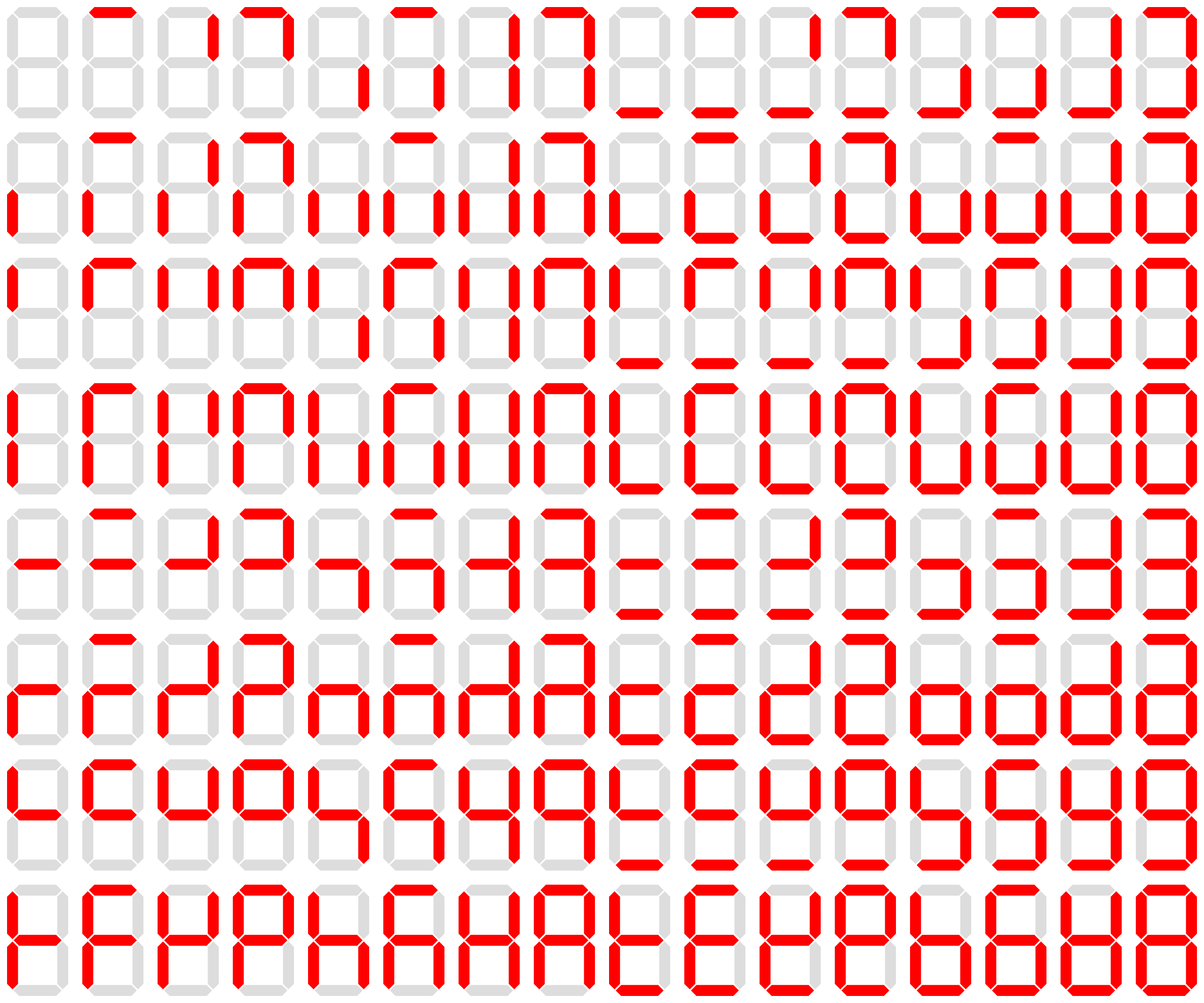
Inspired by 128 possible combinations of 7-seg display
Sketch of main circuit components
Sketch of time unit logistics
Development
There were three main items: Timers/Counters, LFSR, Memory Cells
Timers/Counters
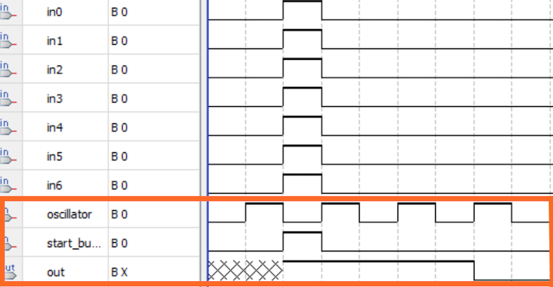
A time circuit is able to control the duration of HIGH and LOW logic levels of other elements in the circuit. In this circuit, the LFSR's output is only to be displayed for 5 seconds.
LFSR
The Linear-Feedback Shift Register (LFSR) allows for pseudo-random bit generation through a seed value and a series of XOR gates that are fed into. This was used to display a psuedo-random pattern.
Memory Cells
Memory cells allow for multi-bit storage via flip flops. By using them, we were able to store both the LFSR's pattern and the user's pattern to ultimately compare them.
Final circuit schematic with smaller circuits compressed into blocks

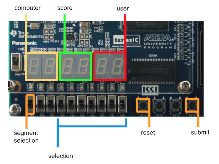
Layout of game UI on DE0 FPGA board

Competed and won award at university's Junior Design Competition
